
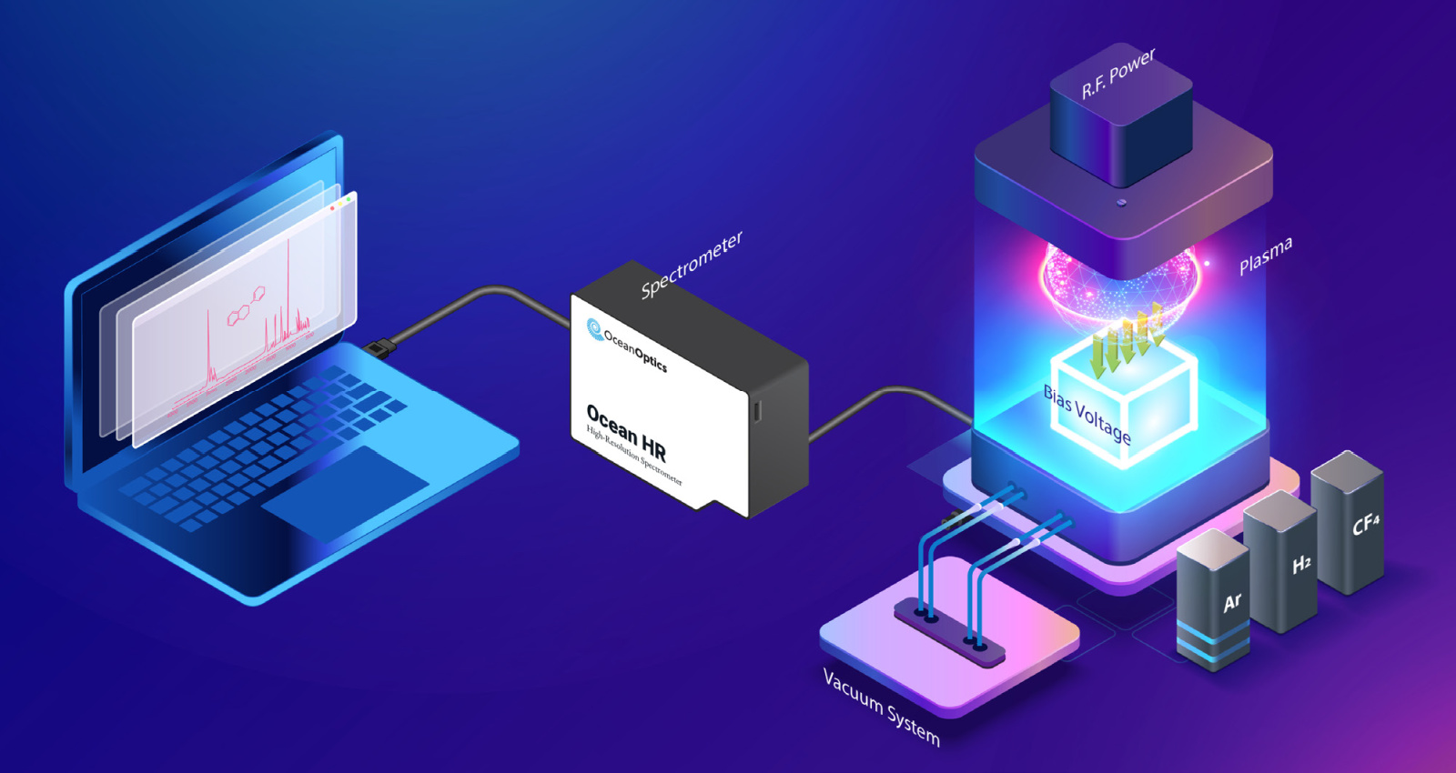
Understanding the Basics of Optical Emission Spectroscopy
Optical Emission Spectroscopy (OES) has become a cornerstone in semiconductor manufacturing, providing a cost-effective and reliable method for real-time, in-situ monitoring of various processes. At its core, OES involves analyzing the light emitted by ionized gases or plasma within the semiconductor fabrication environment. When these gases are excited, they emit photons at specific wavelengths which can be captured and analyzed to provide valuable data on the processes occurring within the fabrication chamber.
Real-Time Plasma Temperature Monitoring with OES
One of the most critical applications of OES is in plasma temperature monitoring. By examining the intensity of emission lines at specific wavelengths, manufacturers can accurately determine the temperature of the plasma. This information is crucial for ensuring that the semiconductor fabrication processes remain within optimal parameters, thereby enhancing efficiency and reducing the likelihood of defects. For instance, monitoring the emission lines of gases like sulfur hexafluoride (SF6) allows for precise control of plasma temperatures using the Stefan-Boltzmann Irradiance equation, ultimately leading to higher quality outputs.
Optimizing Etching and Deposition Processes with Endpoint Detection
In semiconductor manufacturing, the etching and deposition processes are vital for shaping and layering materials. OES plays a significant role in endpoint detection (EPD) for these processes, enabling manufacturers to determine the exact moment when etching or deposition is complete. This precision is achieved by monitoring changes in the emission spectra of gases involved in the process. For example, the use of carbon tetrafluoride (CF4) plasma in etching can be optimized by monitoring the emission lines to ensure that all material has been removed. Similarly, in deposition processes, the ionization of metal atoms in argon plasma can be tracked to ensure that the correct thickness of material is deposited.
Ensuring Clean and Efficient Chambers through OES Monitoring
Maintaining clean fabrication chambers is essential for the efficiency and reliability of semiconductor manufacturing. Residual materials can accumulate during etching and deposition, necessitating regular cleaning to avoid contamination. OES provides a robust method for monitoring the cleanliness of chambers by analyzing the ratio of emission lines of gases like oxygen (O2) and fluorine-based plasmas. A higher O2 to CF4 emission ratio indicates a cleaner chamber, ensuring that the environment is suitable for subsequent fabrication processes. This real-time monitoring capability helps in minimizing downtime and maximizing operational efficiency.
By leveraging the capabilities of Optical Emission Spectroscopy, the semiconductor industry can significantly enhance process control, leading to improved efficiency, quality, and reliability in manufacturing. As the industry continues to evolve towards smaller feature sizes and novel materials, the role of OES is expected to become even more pivotal, driving advancements in semiconductor technology.
Download our white paper now to get all the details and data—no forms to fill out, just instant access! 😉